Getting Started in KiCad
SparkFun Beginner’s Guide to KiCad
KiCAD v5
KiCad FOSDEM 2018: Status & New Features in KiCad 5
CERN
- Open Hardware Initiative (OHI)
- CERN Beams department
- BE-CO-HT section
- Tomasz Wlostowski
- Javier Serrano
- Antonella Del Rosso
- differential pair routing: support fast signals over a long distance and with less noise
- length matching: two signals take exactly the same time to cross the PCB
- Push and Shove router
Open Hardware Repository | Wiki | WorkPackages
KiCad software gets the CERN treatment
Eeschema
[w] = Change to wire mode
Pcbnew
Pcbnew – Reference manual
Drawing Traces
Can I make KiCAD pcbnew NOT place all components at (0,0), Auto-Place

|
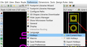
[ESC]         = Cursor
[X]           = Track
[S]           = Set Origin
[SPACE]       = Set Relative Origin
[S]           = Set Grid Origin (manually set in menu "Dimensions" -> "Grid")

[PG UP]       = Switch to Front-Layer
[PG DOWN]     = Switch to Back-Layer
[V]           = Switch between Front and Back
[N]           = Switch Grid to Next
[SHIFT] + [N] = Switch Grid to Previous


Add tracks and vias (wiring):
[Backspace]   = Delete node

Interactive Router (OpenGL):
============================
in normal cursor mode
[X]           = Change to wiring mode
[Left Click]  = Select segment
[U]           = Select trivial connection
[I]           = copper connection

in wiring mode
[D]           = Drag node / track
[E]           = Interactive Router Settings
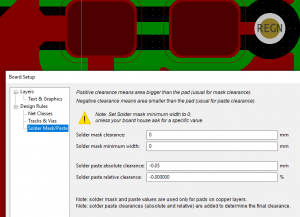
Solder Mask / Paste Setup
 |
Wörterbuch
NPTH = Non Plated Through Hole = nicht durchkontaktiertes Loch
PTH  = Plated Through Hole     = durchkontaktiertes Loch
3D
3D Model
C:\Program Files\KiCad\share\kicad\modules\packages3d
Move exactly
Only available in OpenGL canvas!
“Move exactly” for block selection in pcbnew?
Panelize / Append
Start Pcbnew (stand-alone), not via KiCad!
The “File -> Append Board” menu item is disabled
github.com/madworm/Panelization.pretty, LAYOUT FILES: KiCad footprints useful for PCB panelization (mouse-bites…)
github.com/ThisIsNotRocketScience/GerberTools, Tools to load/edit/create/panelizer sets of gerber files
| pointer tool | |
| fiducial tool | |
| enable high contrast (like hiding all other layers!) |
This is not rocket science: PCB Panelizer & Gerber Tool Suite
Panelization – using GerberPanelizer on Windows (Linux possible)
Panelizing Boards The Easy Way
Panelizing a PCB in KiCad
PCB Design Perfection Starts in the CAD Library – Part 19: PCB Breakaway Panels
PCB Designers Need to Know These Panelization Guidelines
Multiple board outlines don’t render nicely in 3D
Old stuff?
Automated PCB panelization
Panelize Kicad PCB
kicad panelize
Export to STEP
How to share step 3D model with all the components on the PCB too?
KiCad Script Hack for Better Mechanical CAD Export
kicad StepUp script hacks MCAD world!
In Development: 3D Plugins
github.com/easyw/kicad-3d-models-in-freecad
kicad3dmodels
github.com/cbernardo/kicad3Dmodels
Manufacturer: Sullins Connector Solutions
Pad
Eeschema
Multiple Sheet Schematics
Multiple Sheet Schematics in KiCAD
Kicad/eeschema/Hierarchical Sheets
KiCad Hierarchy Tutorial x01 (PDF)
Libraries
KiCad/kicad-library
Kicad Electronic CAD libraries
Quick KICAD Library Component Builder : Component Setup
Wemos KiCad Libraries and Footprints, Lolin32
Arduino Nano library files for kicad
Kicad: librairie Arduino.pretty (for all Arduino types)
github
github.com/niko20010/kicad_libraries, CNY65, etc.
github.com/kiwichrish/kicad_ArduinoNano, Arduino Nano libraries for Arduino Nano
SH_Capacitors.pretty, JST, Molex, USB
ESP32-kiCAD-Footprints, Footprints for the Espressif ESP32 WiFi/BLE Chip and ESP3212 module
github.com/Tinkerforge/kicad-libraries, Verschiedene Footprints, ex. USB Mini mit 3D Modell
FAQ
Question
Electrical Rules Checker
Pin connected to some other pins but no pin to drive it
@(...): Pin 1 (Power input) of component #PWR001 is not driven (Net 24)
Answer
Power pins and Power flags
KiCad: Pin connected to some others pins but no pin to drive it